产品
FIB-SEM
Nanomanipulators
OmniProbeOmniProbe Cryo软件
AZtec3DAZtecFeatureAZtec LayerProbeTEM
Hardware
EDSUltim MaxXploreImaging
软件
AZtecTEM
 牛津仪器集团成员

2nd September 2020 | Author: Dr Pat Trimby
I have always enjoyed attending the annual Microscopy & Microanalysis (M&M) meeting in the US. As a scientist and microscopist it still ranks as the best place to check out all the new technological and commercial developments, with the added benefit that it’s a great opportunity to catch up with a myriad of friends and ex-colleagues who typically attend the meeting each year. Nowadays, as the EBSD product manager at Oxford Instruments NanoAnalysis, it remains the flagship meeting that exerts significant control over our product development timetable. We always want to be able to launch new products at M&M and our time at the meeting is usually spent running back-to-back demonstrations, giving scientific presentations about new technologies and applications, developing networks with other company representatives and, of course, meeting with our customers. It is an expensive, exhausting but ultimately rewarding week.
But not this year. For the first time, M&M was a purely virtual meeting - a step into the unknown for many of us. However, product development still goes on and we, as planned, had 2 major product launches at the meeting: our new AZtecWave Wavelength Dispersive X-ray Spectrometry (WDS) system and Symmetry S2 – a new, faster version of our existing Symmetry EBSD detector, not to mention a new, exciting version of our EBSD data processing software, AZtecCrystal. Now that the dust has settled, we can look back at the meeting and assess how it all went. Is it possible to launch products and run demonstrations on a virtual platform? Are we looking at virtual conferences as an approach that can work well, even in a post-Covid world? Was it as exhausting as a normal M&M week?
As in any normal year, our planning for M&M started pretty soon after the previous year’s meeting finished – we make sure that we have the right booth space reserved, we plan the platform and poster presentations so that we can submit abstracts in time for the February deadline and, of course, we put pressure on our development teams to make sure that our headline products are going to be ready for the Big Show. The sudden arrival of lockdown across the world threw many of these plans into doubt but, unbeknownst to us at the time, it also helped to prepare us for what was to come. We quickly became used to working remotely: development continued at essentially the same pace as before, marketing shifted to more virtual platforms (websites, blogs, webinars and so on) and we developed expertise in remote microscopy and, importantly, in running remote demonstrations. Suddenly the technological foibles of Zoom™, Teams™ and Skype™ were not so daunting, so when it was announced in May that M&M would be held as a virtual conference, we felt confident that Oxford Instruments could still use the meeting to launch successfully our new products.
The months of June and July were frantically spent preparing material for our website, for our virtual exhibition booth and for the presentations that we had lined up, whilst at the same time trying to get detailed information about the format of the meeting. Instead of the live demonstrations that we would normally hold on our own booth at the M&M exhibition, we used 6 microscopes in our laboratories in the UK and US to run remote demonstrations of our new and existing products. Interestingly, over the course of the conference week, we actually gave more demonstrations this year than in previous years, probably in part because we could be more flexible with our timings (although I didn’t envy my colleagues who had demonstrations booked in the 6:00-7:00 am slot). Only time will tell if the impact of remote demonstrations matches that of in-person sessions, but the initial signs are very encouraging.
During the conference we ran some “Spotlight sessions” that focussed on our 2 new products, AZtecWave and Symmetry S2. These were live events, incorporating on-SEM demonstrations, and so were quite challenging given that we had only a strict 30-minute window in which to convey our message. However in both cases we felt that the format worked well, and you can re-watch both presentations and demonstrations on our website.
So what is so special about these new products? For our new WDS system, AZtecWave, it is the intelligent way in which the power of a fully-focussing WDS detector (as used on dedicated electron microprobe systems) is incorporated into the speed and convenience of our latest energy dispersive X-ray spectrometry (EDS) system, AZtecLive. This makes it the only system to achieve true microprobe-WDS spectral resolution on an SEM. We are increasingly confident that the significant work that we have put into the quantification “Tru-Q” algorithms in our EDS software enables us to analyse major element compositions with WDS-precision. However, when there exists a significant X-ray peak overlap or when you need to measure trace element compositions, then you need the resolution and detection power of WDS. As you can see in the aforementioned video, the demonstration showed how trace elements (in this case Si and Co) required analysis using WDS, and how the software guides the user through the set-up of acquisition times, beam current measurement, background signal collection and quantification. In less than 3 minutes, using a combination of both EDS and WDS, the user has measured the composition of this sample to microprobe precision. For anyone used to using our AZtec interface, the layout is instantly recognisable and intuitive, as shown below, bringing WDS-precision to many laboratories that cannot justify the significant expense required to purchase and manage a full electron microprobe microanalysis system.
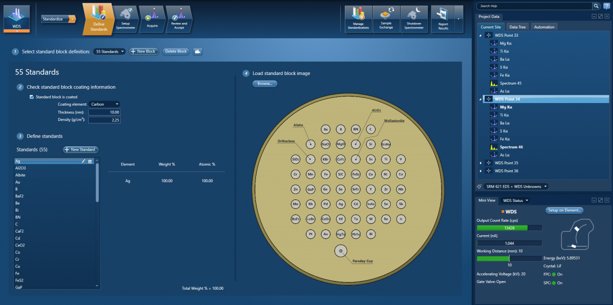
A screenshot of the new AZtecWave user interface, here showing the intuitive layout of the standards definition step. Note the graphical representation of the WD spectrometer status in the “Mini View” to the lower right.
The new Symmetry S2 EBSD detector is all about speed. This system is now capable of analysing samples at speeds in excess of 4,500 indexed patterns per second (pps): to give you an example of what this means in practical terms, we can measure the grain size in samples to international standards in less than 90 seconds! The phase map shown below took 84 seconds to acquire (at 4,725 pps) and, once the twin boundaries have been excluded, contains a total of 2,728 grains - significantly more than the minimum value of 500 grains recommended in various standards, such as ASTM E2627.
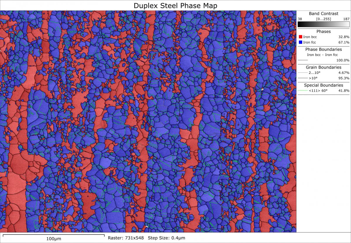
EBSD phase map from a duplex steel sample, collected using the Symmetry S2 detector in only 84 seconds.
However, a key strength of this detector is its sensitivity: the phosphor screen is coupled to the high-speed CMOS sensor using fibre-optics, ensuring minimal loss of signal through the whole analytical process. This ensures that we don’t require high beam currents in order to analyse our samples and therefore don’t compromise on the resolution and performance of the SEM: the data shown in the above image used a beam current of 16 nA, well within “normal” operating conditions for a modern thermal FEG-SEM. If you watch the Spotlight Session video, you will also see that we make quite a big deal about the fact that this is the only genuine “all in one” detector on the market today. We feel that this is a very important facet of the S2 detector: ask anyone who has used EBSD for some time and they will tell you that you never really know what material or analysis type you’ll be confronted with in the future. Having the flexibility in a detector to cope with high angular resolution studies, routine high-speed analyses, extra-large samples or challenging, beam-sensitive materials is a real bonus that will end up saving a laboratory both time and money.
So was the virtual conference a success? During the plenary session on the first morning, when storms in the US had knocked out some internet bandwidth and everyone across the world was having problems viewing the presentations, we all feared the worst. But credit to the Microscopy Society of America and their technical staff, as the teething problems were quickly resolved, and the conference settled into the normal M&M routine of varied platform sessions mixed with commercial events. There were more delegates registered than the previous year, and I feel certain that everyone listened to more talks than ever before, as we could access the presentations in our own time and use the scheduled timetable to connect to the speakers. And, as at a normal M&M, it was still exhausting – the sessions were running late into the evening UK time and I think everyone was pretty drained by the end of the week. But was it as rewarding? Ultimately, I don’t think so – I missed those chance encounters with friends and former colleagues, the lunches with someone you’ve not seen for 5 years or the in-depth discussions with other microscopy vendors about what’s new and what excitement lies just around the corner. Let’s hope we can meet up in person next year in Pittsburgh, but I wouldn’t be surprised if all future M&M’s will have been shaped, at least in part, by the unique experience of 2020.
Somehow missed the swathe of product launches? Sign up to our mailing list to never miss out again!
Sign up nowWe send out monthly newsletters keeping you up to date with our latest developments such as webinars, new application notes and product updates.

© 牛津仪器 2026
 公安机关备案号31010402003473