产品
FIB-SEM
Nanomanipulators
OmniProbeOmniProbe Cryo软件
AZtec3DAZtecFeatureAZtec LayerProbeTEM
Hardware
EDSUltim MaxXploreImaging
软件
AZtecTEM
 牛津仪器集团成员

9th September 2020 | Author: Dr Matt Hiscock
Thin films and coatings are used in a variety of applications across a range of industries including in consumer electronic devices, in solar cells, in medical/pharmaceutical settings, as optical coatings and many more. They may be functional, provide protection or even be decorative. When working with these films there are a couple of key parameters that we are often concerned with – layer thickness and layer composition.
One approach that we could use to understand layer thickness is ellipsometry – a non-destructive and rapid method, but also one that has relatively low spatial resolution and is expensive to run. It is also an approach which can very accurately measure layer thickness, but it does not give results on layer composition. Alternatively, we could consider XRF. This has the advantage that both thickness and composition can be measured in a non-destructive way rapidly, but the analysis is also at relatively lower spatial resolution and expensive. Yet another approach would be to cross section the sample to be measured in a Focussed Ion Beam (FIB) instrument so that a measurement could be made directly in an electron image – this has major advantage of potentially being a very high spatial resolution approach but is also unfortunately time consuming, expensive and destructive.
As such, what we need is an approach which is rapid, can be applied at high spatial resolution, non-destructive and inexpensive. Perhaps unsurprisingly, just such an approach is the subject of this blog - an SEM based technique available within our AZtecLive NanoAnalysis software suite, AZtec LayerProbe.
AZtecLayerProbe is based on Energy Dispersive X-ray Spectrometry (EDS) and fulfils all of the requirements above. It works on the principal that an electron beam hitting the surface of a sample in a scanning electron microscope (SEM) has an interaction volume which extends into the sample, the size of which varies with the accelerating volume that is used. In a standard, non-layered sample, we might not think about this a great deal, particularly if we are working at low magnification. However, in a layered sample, something interesting happens –X-rays are generated from all of the layers contained within the interaction volume , and, can be used to both identify the elements in the layers and how thick the layers are.
LayerProbe works by iteratively fitting a spectrum calculated from a user generated model of the layered structure to an experimentally acquired spectrum . – By fitting the calculated spectrum to the experimental spectrum while varying the unknown layer thickness and composition in the model, the software arrives at the final values. It can do this with up to 7 layers and with layer stacks up to approximately 2μm thick and can work with layers from a micron scale down to less than a nanometre.
Let’s have a look at LayerProbe in action - we’ll consider a simple example.
The sample that we have is a thin film of Al2O3 on a substrate of Si. We know that the thickness of the layer of Al2O3 is somewhere between 40 and 60nm thick – you can try this yourself with the demo data in AZtec. We start off by creating a model of the layer structure – specifying that the substrate is Si and that it is overlain by the Al2O3. We enter in the nominal structure of the sample and the density of the of the Al2O3 layer – you can see what this looks like in AZtec below.
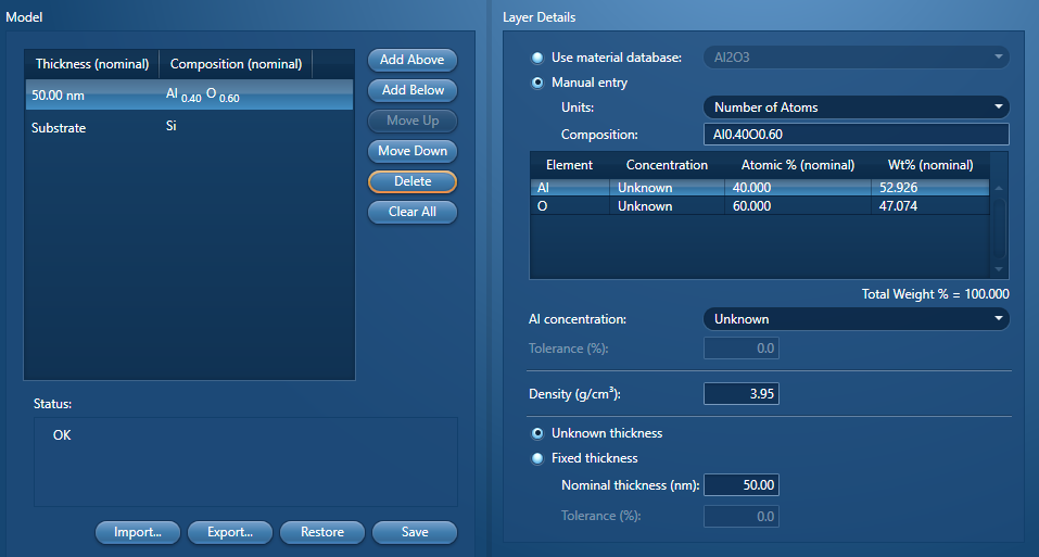
As you can see, I have set up the model with the concentration of the Al and O as unknown and the thickness of the film as unknown. As such, the aim of this analysis is to determine both the film composition and thickness.
With the model created, I can run a simple simulation of the calculation to determine under what conditions it could be solved. This gives me a recommendation of the analytical conditions to use which I can then set on the SEM. It’s then just a case of a beam measurement and acquiring an EDS spectrum from the sample I am investigating.
Once I have done that, I end up with a spectrum like the one below.
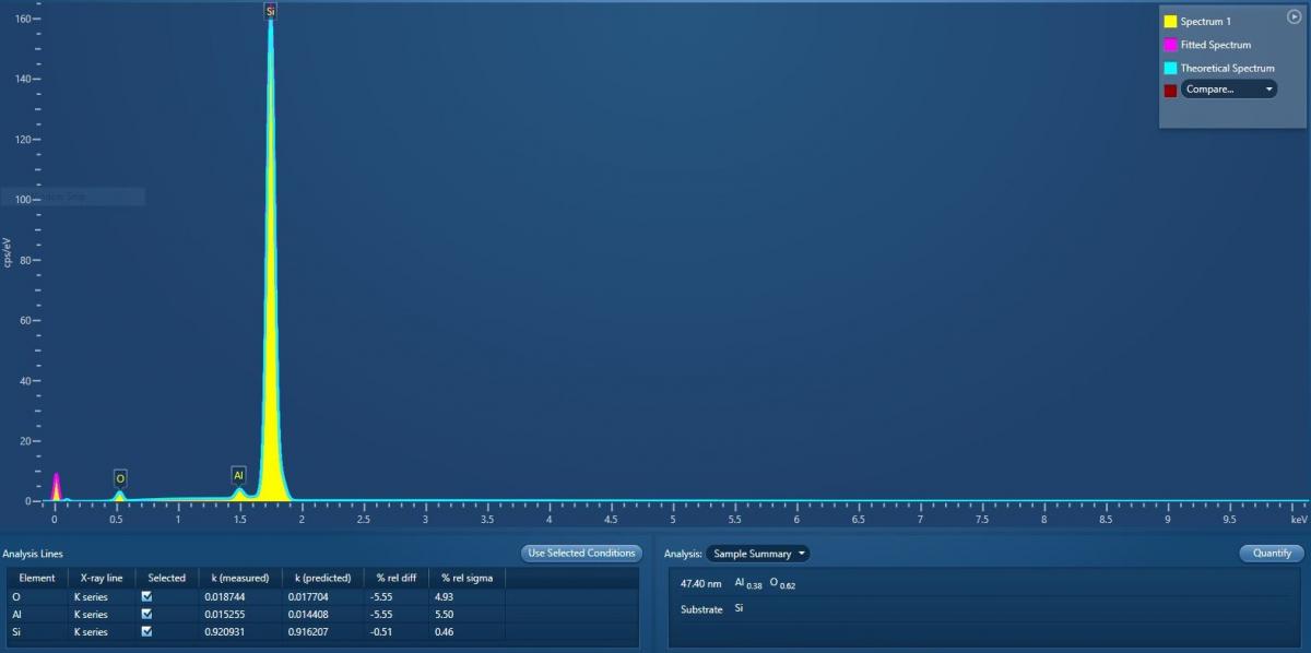
You can see, to the bottom right of the spectrum, that I also have the LayerProbe solution – the thickness of the layer has been calculated as 47.4nm thick and the proportions of Al and O in the layer have been determined to be 38 and 62At% respectively. We also have a measure of the error in this measurement. It really is very straightforward to get a result.
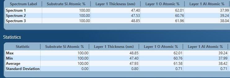
Having done this for one point, the natural tendency is then to go and do it for multiple points across a sample so that we can get an understanding of how the layer thickness and composition varies. In the table below, you can see an example of where we have done this for 3 points across the sample – but you could do this for hundreds of spectra.
And that is it! Essentially LayerProbe is acting as a tool to extract even more information out of your EDS analysis of layered structures, giving you information that is both useful and valuable.
I hope that this brief blog has given you an idea of the capabilities of AZtecLayerProbe. If you have any questions about how it could be applied to your application, please do get in touch and we will do our best to help you.
If you’d like to try LayerProbe yourself, why not download our AZtecTimed licence to run it on your own laptop? We’ll be back later in the year with another blog with more information on LayerProbe including some tips and tricks on how to get the best out of it – join our mailing list to make sure you don’t miss out!
Sign up nowWe send out monthly newsletters keeping you up to date with our latest developments such as webinars, new application notes and product updates.

© 牛津仪器 2026
 公安机关备案号31010402003473