产品
FIB-SEM
Nanomanipulators
OmniProbeOmniProbe Cryo软件
AZtec3DAZtecFeatureAZtec LayerProbeTEM
Hardware
EDSUltim MaxXploreImaging
软件
AZtecTEM
 牛津仪器集团成员

24th February 2021 | Author: Dr Pat Trimby
It is now about a decade since the newly-developed technique of transmission Kikuchi diffraction (TKD) started to generate some interest in the EBSD community. In both 2010 and 2011 a group from the National Institute of Standards and Technology (NIST) in Colorado, USA, headed by Roy Geiss and Robert Keller, presented some interesting results at the annual Microscopy & Microanalysis (M&M) conference. They showed the potential to collect good quality diffraction patterns from nanoparticles and nanowires down to 10 nm in diameter, using conventional EBSD equipment in a standard SEM.
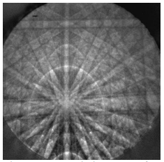
Diffraction pattern from a 30 nm diameter GaN nanowire. Taken from Geiss et al., Microsc. Microanal. 16 (Suppl 2), 2010, 1742-1743.
I think it is fair to say that the technique did not instantly take off. I clearly remember my own introduction to SEM-based transmission diffraction: I was not present at the 2010 M&M meeting in Portland but I was there the following year for the meeting in Nashville. However, at the time I was working in a laboratory in Australia that had just invested in a new FIB-SEM with full 3D microanalytical capability, so I decided to attend a parallel FIB session rather than to hear about this “niche” application of EBSD on electron transparent samples. It was a significant mistake on my part! After returning back to Australia, I received an email from Scott Sitzman (who at the time was Oxford Instruments’ EBSD Applications Specialist in the USA and was one of the authors of the 2011 study) asking what I thought of this new technique. To my shame I had to admit to missing the session, so he kindly sent over some of the results: immediately I realised what a fantastic technique this could be and started asking colleagues if I could borrow some of their TEM samples to see whether we could reproduce the results of the NIST group.
Fast forward to mid-2012 and it became clear that there was another issue with this emerging technique: the name. Geiss and Keller used the name “transmission electron forward scatter diffraction” (t-EFSD) in their 2011 paper but, when publishing in the Journal of Microscopy, the reviewers suggested a change to “transmission EBSD” (Keller and Geiss, Journal of Microscopy, Vol. 245 (2012) pp. 245–251). Some months later I published some initial results focusing on the resolution benefits of orientation mapping using transmission EBSD (Trimby, Ultramicroscopy, Vol 120 (2012) pp 16–24) and was advised by one reviewer that this was nothing more than low-energy Kikuchi diffraction, and that it was “contradictory” to use the term “backscatter” when describing a transmission technique. Hence, I changed the name to “transmission Kikuchi diffraction in the SEM”, meaning we had 3 terms for the same technique: t-EFSD, t-EBSD and TKD. The reviewers have a lot to answer for! All 3 names are still in use today, but “TKD” is generally the most commonly used and the one we use at Oxford Instruments.
The benefits of TKD can be summarised in a single word: resolution. The interaction between the beam (typically at 30 kV) and an electron transparent sample enables a significantly better spatial resolution than can be achieved using conventional EBSD on a bulk sample. Routinely it is possible to demonstrate a resolution of 5-10 nm, and this has been confirmed in numerous subsequent publications. This makes the technique ideal for characterising nanomaterials (i.e. samples with structures below the 100 nm scale) but, importantly, it is also ideal for analysing heavily deformed materials (samples with very high dislocation densities). Recently we posted on social media a TKD map that I collected a few years ago showing an ultra-fine grained shear band in a heavily deformed Al alloy and this has become one of our most liked and commented social posts. Interestingly one of the comments suggested that the image would make a good jigsaw puzzle – I would definitely agree with this but can confirm, based on personal experience, that you need a good deal of patience!
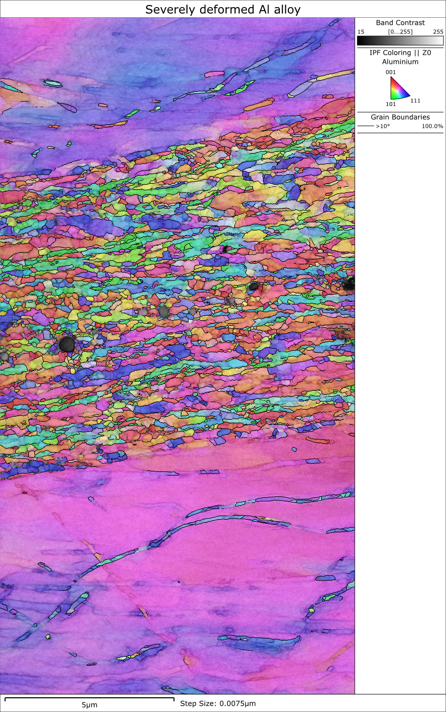
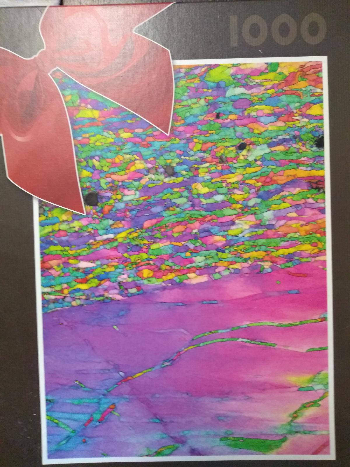
TKD orientation map of a nanoscale shear band in a deformed Al alloy – perfect for a jigsaw gift.
At Oxford Instruments we understand that one of the key benefits of TKD in the SEM is its ease of use. It works beautifully with your standard AZtec EBSD software and any of our CMOS-based EBSD detectors, so there is no need to swap detectors or to change the configuration of your regular EBSD system. We already have an optimised band detection routine that was developed to cope with the broader Kikuchi band widths that are typical when in the geometry required for TKD (and, as I mentioned in a recent blog, this band detection routine works best for all conventional EBSD analyses as well); however, there is more to come. We are currently working on improving the ease of analysing using TKD within AZtec, so watch out for some developments in this field in the next software release, and we have also been looking into removing some of the sample preparation obstacles. For many metals and alloys applications (such as in the deformed Al alloy example above), electropolishing standard 3 mm TEM discs is still the best approach and provides a large, electron-transparent region. However, for more challenging samples it is often best to prepare them using a FIB-SEM. We have been working on a new approach to TKD sample preparation in the FIB-SEM, enabling rapid preparation without the need for any liftout. Our initial results, which we expect to publish in the coming months, indicate that the whole process can be completed in less than 30 minutes, making this wonderful branch of EBSD even more attractive to researchers exploring the nanoworld.
It was fun to be involved in the early stages of TKD development, but I hope that the next decade will be even more exciting, marking the transition of TKD from a niche tool to a mainstream nanomaterials characterisation technique accessible to many more of our customers. Now that really would be progress!
We send out monthly newsletters keeping you up to date with our latest developments such as webinars, new application notes and product updates.

© 牛津仪器 2026
 公安机关备案号31010402003473