产品
FIB-SEM
Nanomanipulators
OmniProbeOmniProbe Cryo软件
AZtec3DAZtecFeatureAZtec LayerProbeTEM
Hardware
EDSUltim MaxXploreImaging
软件
AZtecTEM
 牛津仪器集团成员

23rd July 2020 | Author: Dr John Lindsay
When it comes to in situ FIB liftout, there are many things to consider, one aspect which is often overlooked is the grid you attach your liftout sample too. The majority of FIB users use a standard grid. This is inevitably copper, usually with 3 posts. However, there are many alternatives available with different materials and designs, each with its own advantages.
The number of posts on a grid is primarily an indication of how many samples you can attach. More posts, more samples (but narrower posts). I prefer not to attach multiple samples to a single grid, to minimise theof damage when manually handling the grid. However, I do use multiple post grids as they give a redundancy against damaged/misaligned grids and samples lost due to over thinning. There are 2 post designs: flagpole and V notch. Both suited to different attachment methods and applications.
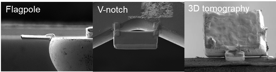
Examples of common lift out attachments for FIB and P-FIB
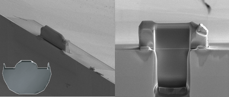
Copper grids are the most popular, due to them been relatively inexpensive and offering a smooth surface for attachment. They also provide flexibility for different attachment approaches with their different post designs. Being copper and <50um thick, they do need care when handling. There are 2 variations of most Cu grid designs, created by different manufacturing processes (identifiable by the downset value of the Cu grids). Visually both grids are similar (see photo below), but the sharpness of the edges commonly used for attachment are different (see electron image of the V post from each grid, the difference is most noticeable at the base of the post), while both are suitable for lamella preparation the more defined shape simplifies the process.
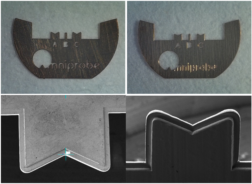
Left “Standard” grid compared to right a “shallow downset” grid
Molybdenum grids are similar in design to the Cu grids (available in 3-post and 4-post configurations) and are suited for EDS analysis of Cu-containing samples. These grids are challenging to fabricate and present a more textured surface compared to the Cu grids. In some cases, you may need to FIB mill small burrs to achieve a smooth flat attachment surface. I recommend using the 3-post grid when a V post is required, as v notch on a 4-post grid is shallow, as seen below.
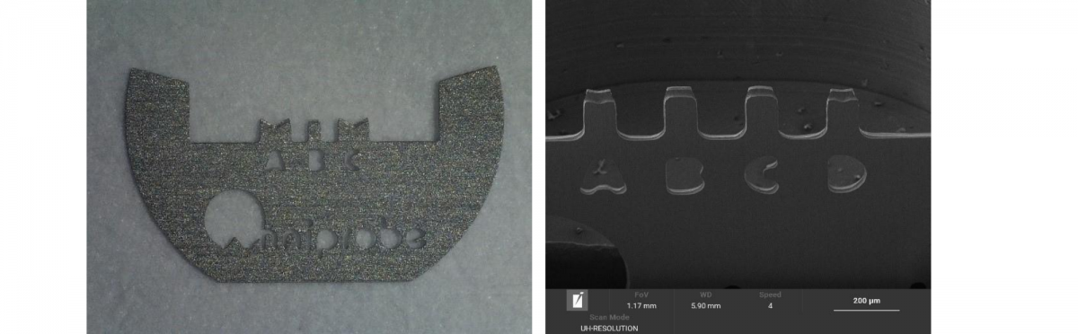
Images of 3 and 4 post Moly grids
Beryllium provide the lowest background EDS signal. However, fabrication is limited due to the materials properties, as such these grids are only available as a half ring.
The final grid available is Silicon. Silicon grids are ideal for silicon semiconductor devices as the grid mills at the same rate of the devices matrix and introduces no additional elemental contamination. They are significantly different from traditional OmniGrids. There are 2 main designs, bevelled and shapable fingers. As silicon mills quickly the finger design is intended to be customised to match you sample and application, atom probe tomography . The bevel design is angled to match the angle of a conventional undercut. This provides a fast, simple way to attach a sample by multiple points (see advantages of the V-notch). The grids are ~ 100 mm thick which makes them more rigid compared to the metal grids and easier to handle, particularly important for cryo applications. The removal of the fingers on the bevelled grids also benefits cryo as the deposition used to attach the sample is not shadowed by the grid post.
Bevelled silicon grid, shows matched milling rate to silicon wafer sample attached
Hopefully this brief introduction has given you a valuable insight into the value of each of the different grid types and will allow you to select the best grids for your needs from our e-store which is stocked with a variety of options to suit every application.
We send out monthly newsletters keeping you up to date with our latest developments such as webinars, new application notes and product updates.

© 牛津仪器 2026
 公安机关备案号31010402003473