产品
FIB-SEM
Nanomanipulators
OmniProbeOmniProbe Cryo软件
AZtec3DAZtecFeatureAZtec LayerProbeTEM
Hardware
EDSUltim MaxXploreImaging
软件
AZtecTEM
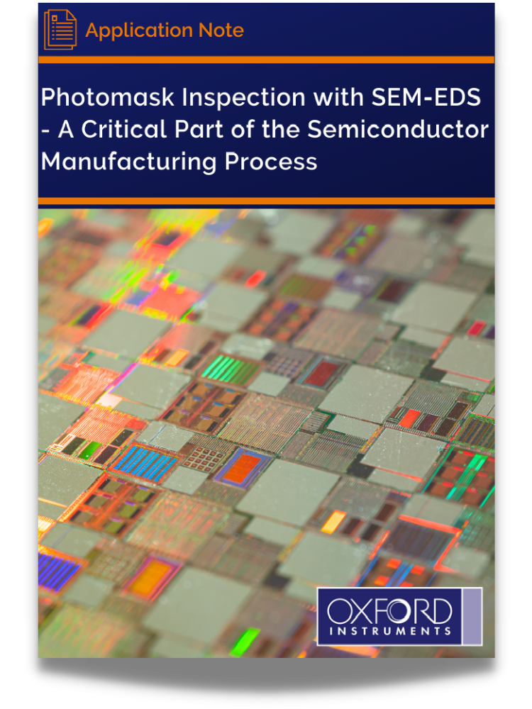
A photomask is a stencil for printing patterns on a wafer during the semiconductor device manufacturing process; it contains the patterns used to create integrated circuits and can be used to manufacture nanoscale features. The photomask must have accurately controlled patterns and zero defects, because mask errors will be amplified and repeated on the wafer. Optical inspection lacks the required spatial resolution, so the electron microscopy EDS inspection is the solution.
By downloading this application note, you will learn how:
 公安机关备案号31010402003473