产品
FIB-SEM
Nanomanipulators
OmniProbeOmniProbe Cryo软件
AZtec3DAZtecFeatureAZtec LayerProbeTEM
Hardware
EDSUltim MaxXploreImaging
软件
AZtecTEM
 牛津仪器集团成员

1st July 2020 | Author: Dr Pat Trimby
You may recall an earlier blog that I wrote giving some tips and tricks for getting the most out of your Symmetry S2 EBSD detector. In that post I focused on the amazing flexibility offered by the software-controlled elevation control and gave some guidelines regarding the best detector mode to use for different applications – you can read that blog here. In this second part, I will give some additional tips for extracting the most out of your Symmetry S2 detector, (including the latest, ultra high-speed version, the Symmetry S2), focusing on the exposure time, collecting forescatter images, and showing the benefits of retracting the detector a little way. These tips are focused on our Symmetry S2 detector but many of the guidelines will be also valid for our complete range of CMOS-based EBSD detectors and, in some cases, even for our older CCD-based Nordlys detector range.
This is a question that I often get asked – “what exposure time should I use?” – and it is difficult to give a precise response. Rarely are 2 samples, or even 2 SEMs, the same and so there will always be variations from sample to sample or from laboratory to laboratory. Additionally, the quality of information that you require from your sample will be a key factor in this decision.
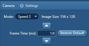
The user interface in the “Optimize Pattern” navigator step in AZtec is relatively simple. Here you can choose the detector mode, set the detector exposure time (as well as gain and frame averaging) and perform background averaging to produce good quality EBSPs.
Setting the exposure time is a simple process: choose the detector mode and then press “restore default” and AZtec will set the optimum exposure time for the current electron dose onto the detector (i.e. just below the saturation level).
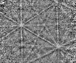
However, often you do not need to work with the optimum exposure time, allowing you to undersaturate the detector and collect data at much faster rates. For example, when analysing a steel sample with about 10 nA beam current on a field emission gun (FEG) SEM, the default exposure will typically be around 2-3 ms. If you reduce this value by an order of magnitude, say to 0.3 ms, then the raw EBSP signal will appear very dark but the background corrected signal will still be good enough for reliable indexing and good quality data. Here is an example EBSP from austenitic steel using such conditions (approx. 10 nA, 0.3 ms exposure):
If your sample contains more weakly diffracting phases (e.g. oxides, minerals, ceramics) or is deformed, then you will not be able to reduce the exposure time by so much, and may even have to increase the exposure time in order to get good quality data. Once again, there are no set rules, but the following diagram shows how increasing the electron dose (here measured as the beam current x exposure time) can improve your results, especially in deformed materials. This example shows a region of high plastic strain in between 2 crack tips in a duplex stainless steel:
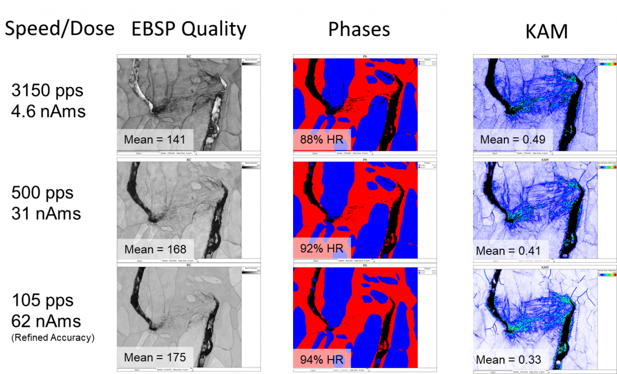
The increase in hit rate as the dose (i.e. exposure time) increases is almost entirely due to better solving of EBSPs in the most highly deformed regions between the 2 cracks. The lower KAM values reflect the improved precision of indexing as the dose increases.
To summarise, you can follow these steps to ensure you get the best exposure time for your analyses:
Forescatter detectors (FSDs) are extremely useful for providing a quick overview of a microstructure, either to help you determine where and how to proceed with any subsequent EBSD analyses, or for providing useful microstructural information in its own right. The Symmetry S2 detector can have up to 5 FSD diodes mounted around the phosphor screen, providing high speed images to show electron channelling (or orientation) contrast, topography, or atomic number (Z) contrast. Key to the nature and quality of the signal is the geometrical relationship between the beam-sample interaction and the detectors, as shown schematically below:
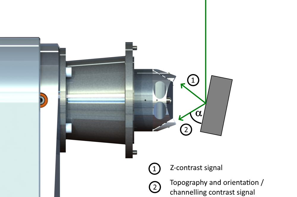
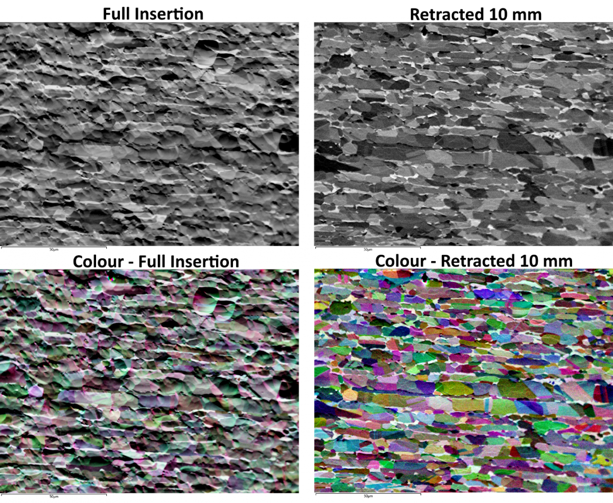
The angle “a” in the image is important in determining the nature of the signal on the lower diodes. If the detector is very close to the sample, or the sample is at a high position relative to the detector (i.e. a is small), then the signal will be dominated by topography. As the detector is retracted (or the sample lowered), the increase in a will enhance the crystallographic signal and decrease the topographic signal. This can be shown in the following example: a duplex stainless steel sample has been polished using a broad Ar ion beam polisher, introducing significant topography. With the S2 fully inserted, the signal is dominated by this topography, whereas retracting 10 mm gives a much more useful image showing the crystallographic variations such as the grain and twin structure. The lower images show the effect on the colour FSD image in AZtec – clearly the slight retraction of the S2 produces a much better image.
To conclude – to get the most informative FSD images, try retracting your detector a little way (5-10 mm is usually sufficient), collect the image, and then re-insert to the optimum position for subsequent EBSD analyses.
We’ve already seen in the previous section that retracting symmetry by 5-10 mm from the full insertion position dramatically enhances the quality of the FSD images. However, EBSD data acquisition can also be improved by detector retraction. As you retract the detector, the solid angle subtended by the phosphor screen decreases and you effectively “zoom” into the diffraction pattern, as shown by the animation below:
In this case the detector is retracted by about 25 mm from full insertion but even just retracting 5 mm will result in significant broadening of the Kikuchi bands. Why might this be useful? For most analyses it is not – the smaller solid angle, the broader bands and the weaker signal all result in a slower analysis with, possibly, a lower indexing rate. However, there are applications where this can be beneficial:
Typically, for such EBSPs we would either use the more precise indexing available using AZtec’s Refined Accuracy mode or else would benefit from processing the EBSPs using 3rd party software (such as developed for so-called “High Resolution EBSD”). The improvements in angular precision or in phase/orientation discrimination will of course be very dependent on the quality of the EBSP, and so the condition of the sample and the set up of the EBSD detector will be very important. However, if you have a sample that gives good quality EBSPs, then switch your Symmetry S2 to resolution mode, retract the detector by a few mm, set up the exposure settings to give good quality patterns, and switch on Refined Accuracy indexing, and you might just extract some better quality data from your samples.
I hope that these 2 Symmetry S2 “tips and tricks” blogs have been helpful to many of you. If you have requests for other similar blogs for any of our products, then please don’t hesitate to let us know. In the meantime, good luck with your analyses and keep enjoying the fascinating world of EBSD!
We send out monthly newsletters keeping you up to date with our latest developments such as webinars, new application notes and product updates.

© 牛津仪器 2026
 公安机关备案号31010402003473