产品
FIB-SEM
Nanomanipulators
OmniProbeOmniProbe Cryo软件
AZtec3DAZtecFeatureAZtec LayerProbeTEM
Hardware
EDSUltim MaxXploreImaging
软件
AZtecTEM
 牛津仪器集团成员

26th March 2019 | Author: Dr John Lindsay
Focused ion beam (FIB) preparation of site-specific transmission electron microscopy (TEM) samples is a well-established method. However, obstacles to making a good TEM lamella remain, common challenges (and the solution, in case you’re in a hurry) faced when trying to prepare a high-quality FIB sample are:
With minor workflow tweaks, these issues can be mitigated to drastically improve sample quality and simplify the operator’s life.
Curtaining is an artefact resulting when different materials, mill at different rates. It is most prevalent in samples where a hard, structured material (with a slow milling rate) is above or inside a soft material (fast milling rate) but also occurs when surface topography or voids (such as a crack) are present. On a cross-section, curtaining prevents good analysis, in TEM lamella preparation the thickness variations are catastrophic.
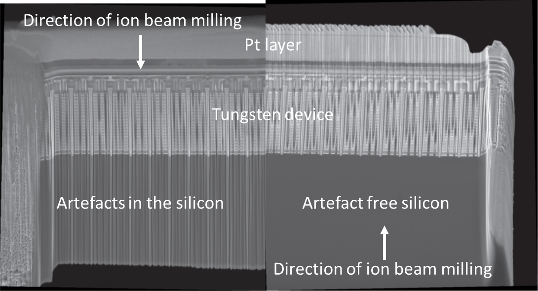
Left: image shows the detrimental effect curtaining has when milling a typical semiconductor device, consisting of metal (tungsten) features above a silicon matrix. In cross-section the curtaining produces artefacts in the silicon, the presence of these artefacts when attempting to thin the sample to electron transparency, will results in sample disintegration.
Right: how the device should look, milling artefacts are present, but only in the Pt layer, not the device.
Curtaining can be minimised by optimising the milling direction. This typically means changing the orientation of the sample so that a uniform layer mills first, this will produce less curtaining. In this example, it requires inverting the sample so the silicon layer mills before the tungsten. During lamella lift-out, this can be achieved using an OmniProbe with the capability to rotate the sample in the chamber. However, rotating a lift-out sample on an OmniProbe tip by 180° will not invert the sample as all manipulators are mounted on at an angle relative to the sample. This challenge can be visualised (without needing a FIB) by rotating a post-it note (lamella) attached to a pencil (probe).
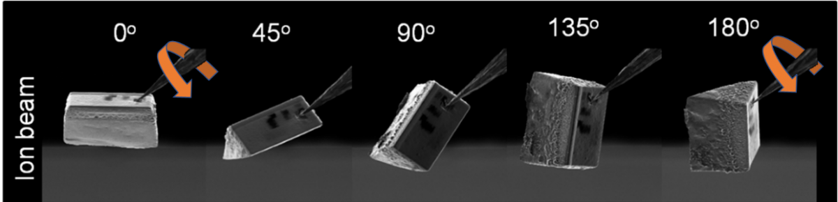
Sequence of ion beam images showing a sample rotation of 180° with an OmniProbe
To achieve sample inversion a combination of angles (probe and stage) can be calculated to create microscope specific recipes for vent free creation of a plan view sample (a sample rotated by 90°), combining this recipe with an OmniPivot (a TEM grid holder, which can pivot the grid without directly handling the grid) produces sample inversion. The result is a high-quality sample with minimised milling artefacts. The combination of an OmniProbe and OmniPivot means that almost any orientation sample can be created.
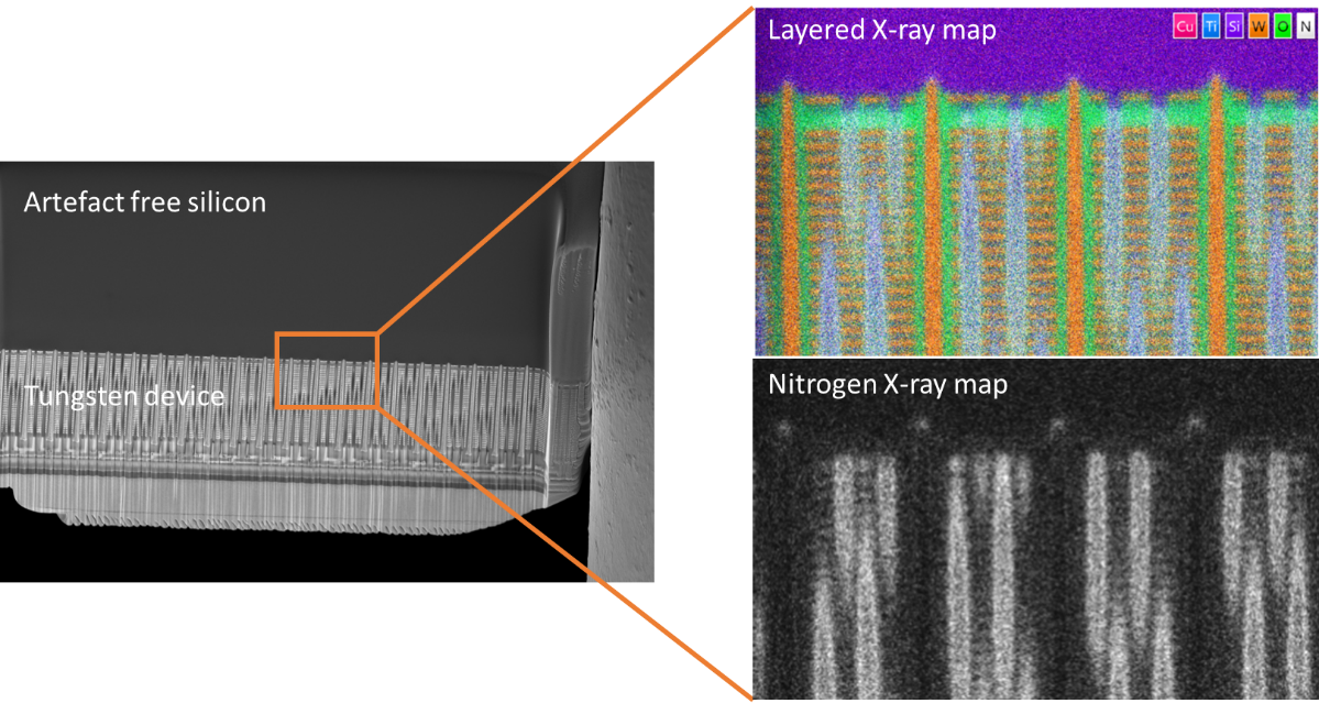
Same semiconductor device as above but inverted before milling. The silicon is artefact free, enabling the high-resolution EDS map acquired with an Extreme X-ray detector, to identify nitrogen at the bottom of the tungsten via’s.
Damage resulting from the interaction between the Ga ion beam and sample is well documented. This damage can include phase transformation in stainless steel and grain growth in thin films. Optimised milling parameters to minimise these effects are documented, but the effect of ion beam imaging during sample preparation is often overlooked.
To minimise the sample exposure to the ion beam, lift out can be completed normal to the ion beam (tilted relative to the electron beam). This is beneficial for beam sensitive samples, as it:
The challenge for this lift-out method is the ability to match the manipulator's movement to the tilted samples X, Y, Z coordinates, a standard feature with all OmniProbes.
The final challenge faced when preparing high-quality TEM samples is to optimise the lamella thickness. Insufficient thinning wastes both TEM and FIB time, over thinning destroys the sample wasting FIB and prior sample analysis. There is a range of imaging methods which are applied when thinning a lamella, but they require both knowledge of the sample and an experienced operator.
AZtec LayerProbe has been demonstrated to give accurate measurements of lamella thickness including details of ion beam damage and redeposition contamination, So the ‘guesswork’ can be removed from thinning a lamella and the sample quality can be guaranteed before expensive TEM analysis.
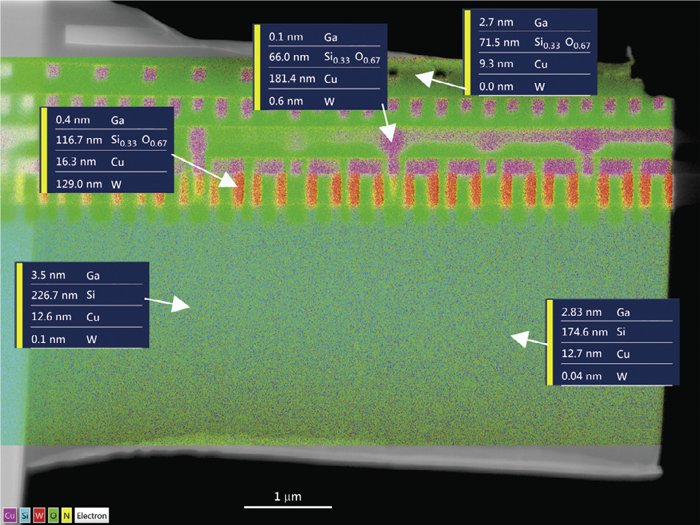
TEM sample showing with AZtec LayerProbe results from different parts of the sample, indicating sample thickness, Gallium implantation and Cu redeposition.
For details on how to measure lamella thickness with LayerProbe or to find out more on these applications, visit our Application Note Library.
We send out monthly newsletters keeping you up to date with our latest developments such as webinars, new application notes and product updates.

© 牛津仪器 2026
 公安机关备案号31010402003473