TEM中的半导体成像-实时解决峰值重叠问题
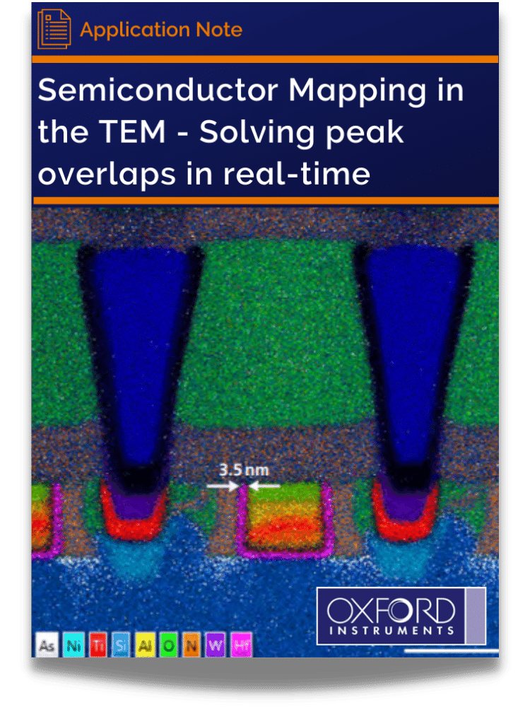
Development and testing of semiconductor devices requires extensive knowledge of local structure and elemental composition. With feature sizes of <5 nm, it is often necessary to perform imaging and EDS analysis in a S / TEM. Once in the TEM, there are still many difficulties to be overcome to acquire accurate elemental maps. Elemental analysis of semiconductors is typically difficult due to strong overlaps of X-ray lines between commonly used elements and low concentrations of dopants. Not only are concentrations of dopants small but their X-ray lines often overlap with other materials used in semiconductor processing. This brief shows how AZtecTEM solves these overlaps to achieve an accurate elemental analysis.
点击下载应用报告
 牛津仪器集团成员


 公安机关备案号31010402003473