产品
FIB-SEM
Nanomanipulators
OmniProbeOmniProbe Cryo软件
AZtec3DAZtecFeatureAZtec LayerProbeTEM
Hardware
EDSUltim MaxXploreImaging
软件
AZtecTEM
 牛津仪器集团成员

28th July 2021 | Author: Dr John Lindsay
FIB-SEM is a relatively common method of preparing a sample, for both SEM and TEM analysis. When preparing a sample with an ion beam, there are multiple aspects to be considered if a good sample is to be produced. A good sample is often considered one which images well (no obvious artifacts from sample preparation), but this is not the only consideration when it comes to analytics. Here I will give a few examples of how FIB preparation can impact analysis, along with some advice on how to mitigate the impact.
The most obvious effect when FIB preparing a sample is curtaining. Curtaining can occur when a sample has different materials with variable milling rates. It is considered undesirable, as it creates imaging artifacts and, when preparing a TEM sample, limits the archivable sample thickness. When it comes to analytical analyses, the topography associated with curtaining can result in shadowing and the absorption of low energy peaks.
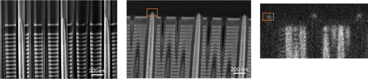
Fig. 1 Left: sample prepared by conventional milling with curtaining; Centre: sample prepared by backside thinning to avoid curtaining; Right: nitrogen EDS map from backside thinned sample.
In the example above we have the same sample prepared with and without curtaining in the region of interest (details on how this was achieved can be found here). EDS mapping of the sample with an Ultim Extreme showed a concentration of nitrogen at the tips of the Tungsten Vias (indicated in the orange box). Performing the same analysis on the curtained sample resulted in this nitrogen concentration not been observed. Common methods used to mitigate curtaining are changing the sample orientation, depositing a protective layer, and milling with a reduced ion beam current.
Another potential effect of ion milling on EDS analysis is contamination. Contamination occurs when ions used to mill are implanted, or the milled material redeposits on the sample. Redeposition is typically observed at (but not limited to) the bottom of a cross-section. The redeposited materials composition is a combination of the milled material (from the sample or a support structure like a liftout grid) and ions from the ion beam. The example below (fig. 2) shows gallium contamination of solid-state lithium-ion battery (contains no gallium). In the cross-sectional EDS map, a significant amount of gallium is observed at the bottom of the cross-section, but importantly not at the top in the particles being analysed.
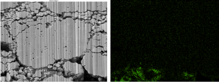
Fig. 2 Cross section of lithium ion battery. Redepostion is observed at the bottom of the cross-section. This can be seen in the EDS map for gallium (which is not present in the material)
Redeposition can be minimised by avoiding over milling (to avoid milling the material below the surface on interest) and using less aggressive conditions in the final steps of preparation. Another issue of note; if you’re looking at a sample containing copper, copper liftout grids should be avoided.
It is not just the chemistry of a sample which can be affected by ion milling, the crystal structure can also be impacted. A well-known example of this is the amorphization of silicon. The EBSD signal images in fig. 3 were taken from the same crystal of silicon, however one was taken after been polished at 30 keV and 500 pA (no Kikuchi pattern produced), the other at 5keV and 500pA (clear Kikuchi pattern). The lack of a pattern is not because of the detector, but because EBSD is a surface sensitive technique, and the surface has been amorphized meaning no patterns are generated.
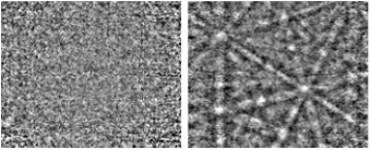
Fig. 3 Pattern acquired from a single crystal of silicon, left after ion polishing at 30keV 500pA, right after 5keV 500pA. Both extracted from the same map, which was acquired using 20 keV and 1 nA e-beam.
In addition to destroying crystal structure, ion beam interactions can also change the phase; a common example of this is austenitic stainless steel (SS). The image below (Fig. 4) shows EBSD maps from an austenitic SS with 3 regions exposed to different ion beam doses. The different doses were achieved by imaging the regions perpendicular to the ion beam for 30s, 20s and 10 seconds (using a 30keV, 1 nA beam and 300 nS dwell time). The regions with a higher dose have undergone a phase transformation from austinite to ferrite, yet in the low dose region, the phase is unaffected.
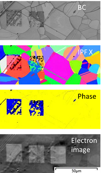
Fig. 4 Band contrast, orientation, and phase maps (austinite yellow, ferrite blue) with corresponding electron image. Three regions were exposed to a 30 keV, 1 nA. Ion beam exposure times decreased left to right.
When it comes to avoiding crystallographic damage, the ion beam accelerating voltage is key, with low voltages been less likely to produce damage. Though as the SS example above shows, dose is also an important factor.
Whilst I have shown examples of how ion beams can damage a sample; these effects are rare and often can be avoided/mitigated with care. When working with a new material or ion source (examples shown are all from a Ga FIB), it is important to understand how they interact. The use of EBSD and EDS enables the interactions to be quantified, in addition to characterising the produced sample.
We send out monthly newsletters keeping you up to date with our latest developments such as webinars, new application notes and product updates.

© 牛津仪器 2026
 公安机关备案号31010402003473