产品
FIB-SEM
Nanomanipulators
OmniProbeOmniProbe Cryo软件
AZtec3DAZtecFeatureAZtec LayerProbeTEM
Hardware
EDSUltim MaxXploreImaging
软件
AZtecTEM
 牛津仪器集团成员

22nd April 2020 | Author: Dr John Lindsay
Additive manufacturing has the potential to reduce the quantity of material required to manufacture a component, reduce component production time, and consequently reduce costs. The journey to unlocking that potential is one that follows a familiar route – using material analysis techniques that have already proved their value on conventional manufacturing processes like Electron Backscatter Diffraction (EBSD).
In the aerospace industry the alloy Ti64 (a titanium alloy with ~6% Aluminium and ~4% Vanadium) is widely used. The mechanical strength of Ti64 is closely related to its microstructure, so it is critical to understand the differences between traditionally manufactured components and those produced using additive manufacturing. Only by understanding the component microstructure can we ensure that there is no reduction in part quality.
The microstructure of Ti64 changes at elevated temperatures from a hexagonal closed packed (hcp) crystal structure to the body centred cubic (bcc). At the same time, grain growth occurs during heating. The anneal time, heating rate and cooling rate all effect the final microstructure. In conventional manufacturing heat treatments are used to optimise the microstructure for a specific application. In additive manufacturing sequential layers of material are added to create a near-net shape – a shape that is very close that required for the final product, meaning only minimal surface finishing is needed. These layers can be formed by selective melting of a powder bed or direct deposition of the metal by a welding based process. Both these methods produce cyclic heating and large thermal gradients, the result of which is a heterogenous microstructure which evolves across the component. Through carefully controlling the melt process, the final microstructure can be manipulated to reduce the requirement of additional heat treatments.
To better understand the formation of the microstructure of additively manufactured Ti64, the material is studied at the temperatures where the changes occur. This enables us to observe the changes in real time The evolution of the microstructure during these phase transformations can be imaged and quantified using modern CMOS EBSD cameras such as our Symmetry detector. EBSD measurements at high temperatures require an infra-red (IR) filter in order to block the infrared radiation generated by the sample as it is heated. The effect of the IR radiation is shown in figure 1, where the background signal on the EBSD detector was measured with the electron beam turned off (no signal expected), but with a sample of silicon heated in the microscope chamber to 900oC. The beam-off background signal is shown with and without a IR filter on the detector.
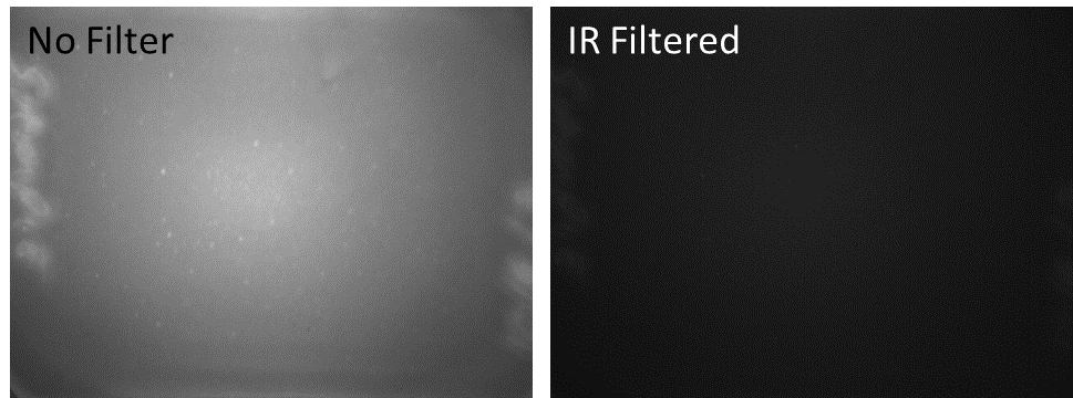
Figure 1: Background signal detected on the EBSD detector with (right) and without (left) an IR filter when a sample of Si in the chamber heated to 900oC and the electron beam turned off.
The low background noise due to the filtering of the IR radiation and the low noise characteristics of the detector means that clear Kikuchi patterns are observed even when a sample is heated to 1000oC. Figure 2 shows patterns obtained from a Ti64 sample at room temperature and ~1000oC. As the sample was heated up, the phase transition from HCP to BCC occurred at ~980oC.
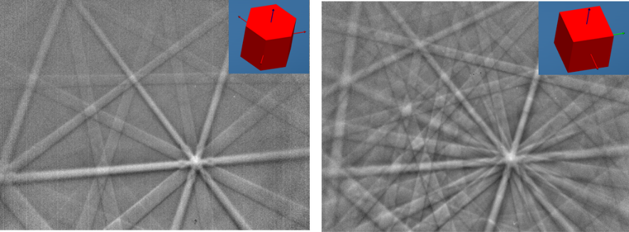
Figure 2: Kikuchi patterns obtained from Ti64 below 980oC and above 980oC showing that the crystal structure of the Ti64 had changed
The ability to acquire data at high speed and low noise with our Symmetry detector is important in this context. High speed offers an even greater insight into the material phase transformations as it enables faster heating and cooling rates to be studied in detail. Additively manufactured materials such as Ti64 experience rapid heating and cooling in the manufacturing process. As a consequence we can better understand complex crystallographic relationships such as between HCP to BCC during heating and cooling cycles. Figure 3 shows an example of this, acquired a region of Ti64 at RT and 1000oC, show radically different phases and grain sizes.
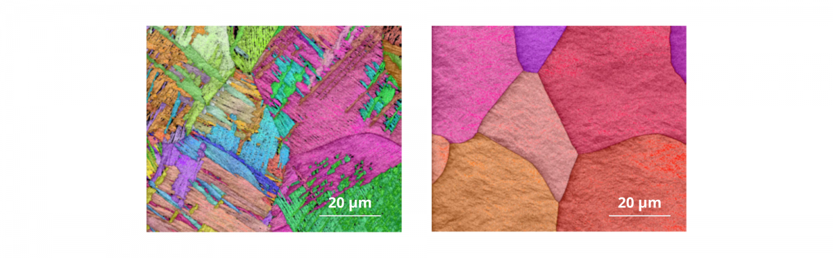
Figure 3: EBSD map acquired from the same region of Ti64 at room temperature (left) and at ~1000C (right). At RT the Ti64 is 99% HCP, while at 1000oC it is transition to 100% BCC phase
Additive manufacturing offers great promise but delivering on that promise requires a deep understanding of the material from powder to product. AZtecAM, our software solution, means the powder products can readily inspected to a high standard and the improved understanding of the process by characterisation means reliable off-the-shelf AM machines can be developed. This opens up new possibilities such as digital inventories - the idea that spare parts can be e-mailed as a design file rather than shipped around the world from a warehouse. It also means products can be repaired, even when they have not been manufactured for years.
To gain a better understanding of how our products and solutions can aid the development of additive manufacturing processes watch our recent webinars on hot stage EBSD and additive manufacturing of Ti64.
We send out monthly newsletters keeping you up to date with our latest developments such as webinars, new application notes and product updates.

© 牛津仪器 2026
 公安机关备案号31010402003473