产品
FIB-SEM
Nanomanipulators
OmniProbeOmniProbe Cryo软件
AZtec3DAZtecFeatureAZtec LayerProbeTEM
Hardware
EDSUltim MaxXploreImaging
软件
AZtecTEM
 牛津仪器集团成员

12th December 2019 | Author: Dr Sam Marks
M2T is much more than just TEM quantification, it is a process that allows you to measure the thickness of TEM samples directly from your EDS spectra. This may sound rather trivial, but in reality, this was previously only achievable via EELS (a technique that can cost up to $1,000,000) and opens up a new dimension to your analysis. A new range of applications, beyond simply measuring the thickness of a sample, can also be undertaken, for example analysis of defect density or dislocation density.
The knowledge of the thickness of a sample also has a huge ramification on the accuracy of your quantification. This knowledge allows you to correct for absorption within your TEM lamella, a large unknown in TEM quantification. Ttherefore, by solving an unknown that is often approximated, we can guarantee a more accurate measurement. More information on this will follow in a future blog post.
We have designed an easy to use process that allows you to achieve this measurement. All you need is the assistance of an Oxford Instruments SI3N4 (silicon nitride) reference sample and the knowledge of the density of the material being analysed.
Once you are armed with these two vital components, the process of calculating the thickness of a sample can be broken down into 3 easy steps:
Acquiring EDS spectra from a Si3N4 reference is the backbone of the M2T process, as this allows AZtec to characterise both the EDS detector and the electron beam. This removes the need for a beam current measurement and allows us to quantify the efficiency of the detector, solving two important variables in the TEM quantification equation. There are no defined acquisition settings for this step but the beam settings used for acquisition, i.e. spot size and aperture, must be the same beam settings used when acquiring the EDS spectra from your sample.
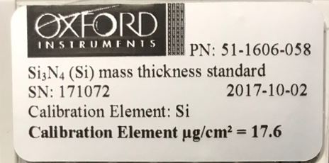
The Si3N4 reference sample supplied by Oxford Instruments
For M2T to work we require the input of two variables: the Calibration Element Mass Thickness value (in µg.cm2), and the density of the material being measured (in g/cm3). The Calibration Element Mass Thickness is precalculated and readily available on the reference sample box, precalculated for each individual pack of reference films. This value is a combined measurement of the density, thickness, and wt% of Si within the Si3N4 film.
The second value and only variable in this process is the density of the material being measured. If it is unknown, then users could acquire EDS from a nearby region of known density, a common example being Pt or C deposited during FIB preparation. This will give the user a thickness approximation, though FIB lamellae are well documented to be wedge-shaped therefore it is advised to acquire the data as close to the region of interest as possible. An approximation of the density can also be used, leading to an approximate value for the thickness of a sample.
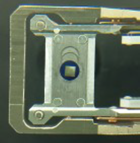
A wedge-shaped specimen of Inconel 600 (Fe8Cr16Ni74, wt%) prepared by FIB. The intended wedge angle is 0.5° +/- 0.07°
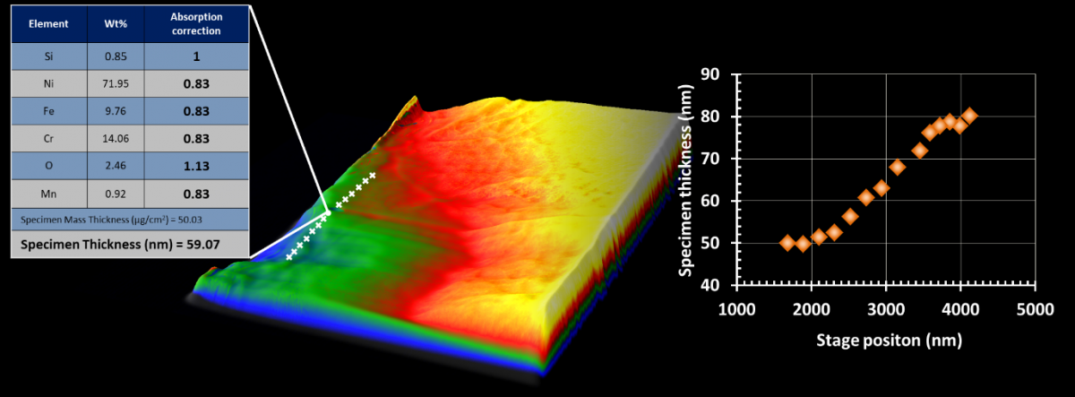
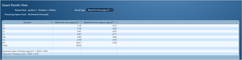
Swapping out the reference sample for your sample of interest, you need to ensure that the microscope is set up in the same beam configuration as that used for the reference sample measurements. You then have the freedom to acquire EDS data from your sample with the Specimen Mass Thickness and Specimen Thickness automatically calculated for each acquired spectrum. This data is readily available for each individual EDS measurement and can be seen in the Quant Results View in the Calculate Composition tab (shown below).
The reported Mass Thickness area of the sample of Inconel 600 (Fe8Cr16Ni74, wt%) observed in the previous figure
With this easy to use process, M2T adds an extra dimension to your TEM with the ability to analyse the thickness of samples. To learn more about AZtecTEM – our newest software solution, powering M2T quantification. View our recent webinar ‘The latest developments in EDS hardware and software technology for the TEM’.
We send out monthly newsletters keeping you up to date with our latest developments such as webinars, new application notes and product updates.

© 牛津仪器 2026
 公安机关备案号31010402003473