产品
FIB-SEM
Nanomanipulators
OmniProbeOmniProbe Cryo软件
AZtec3DAZtecFeatureAZtec LayerProbeTEM
Hardware
EDSUltim MaxXploreImaging
软件
AZtecTEM
25th August 2021 | Author: Dr Sam Marks
Optimising SEM imaging for the observation of features in the surface of a sample often requires users to reduce both their accelerating voltage and working distance. Performing good EDS analysis in these conditions can be difficult, since a conventional EDS setup would typically have a working distance greater than 10mm and a standard accelerating voltage of 20kV.
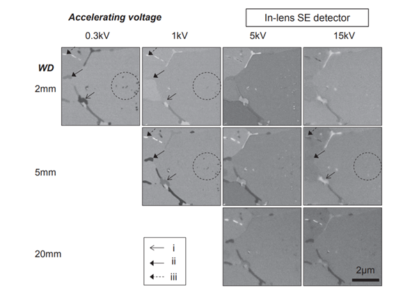
A good example of the importance of optimising SEM imaging conditions was shown by Dr. Sato from JFE-Tec whilst analysing inclusions in steel. During the analysis, Dr. Sato identified a phenomenon in his SEM images where different combinations of working distance (WD) and accelerating voltage changed the contrast of many of the visible features. His findings, highlighted below in Figure 1, indicated that different carbide phases are illuminated with different levels of contrast depending on what combination of accelerating voltage and WD are used in the SEM. Typically greater contrast was observed when using lower accelerating voltages in combination with a reduced working distance, he has named this “The Imaging Sweet Spot”.

Figure 1. In-lens SE images of the same region of the 2.25Cr-1 Mo steel specimen obtained using accelerating voltages of 0.3, 1, 5 or 15kV and WDs of 2, 5, or 20 mm. doi:10.2320/matertrans.M2019078
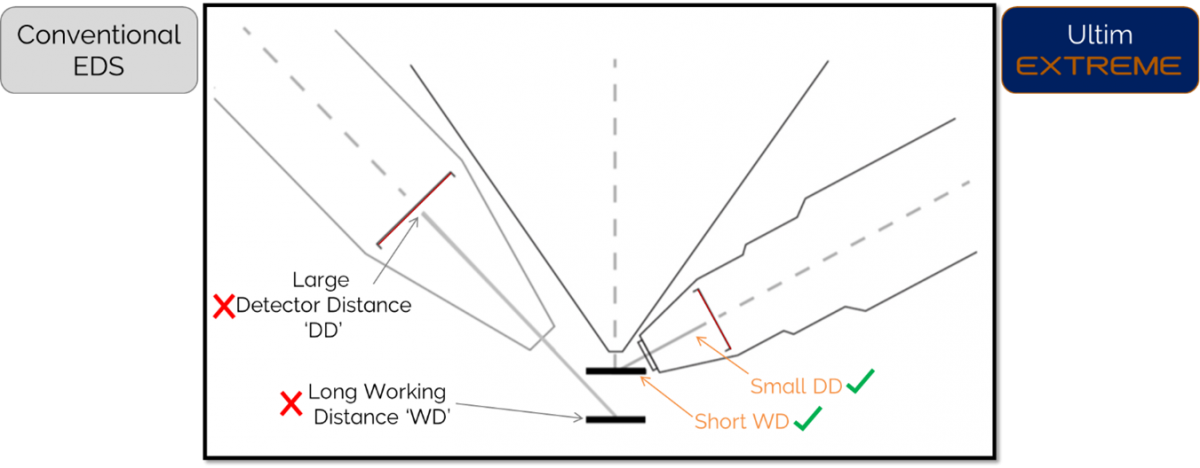
It is possible to use a conventional EDS detector when imaging samples at the imaging sweet spot, but since a standard EDS detector is configured for long working distances and high accelerating voltages the x-ray yield is greatly reduced in this geometry. These issues are resolved by utilising the Ultim Extreme detector, which has been designed specifically to operate at a short working distance using a smaller electron trap to maximise the x-ray counts collected by moving the sensor closer to the sample (Figure 2). With Ultim Extreme we can operate at the Imaging Sweet Spot, with no performance loss and because of its windowless construction it further enhances detection of the light elements that are often found in inclusions and surface particulates.

Figure 2. A comparison between conventional EDS and Ultim Extreme, highlighting the shorter working distance achievable with the Extreme detector.
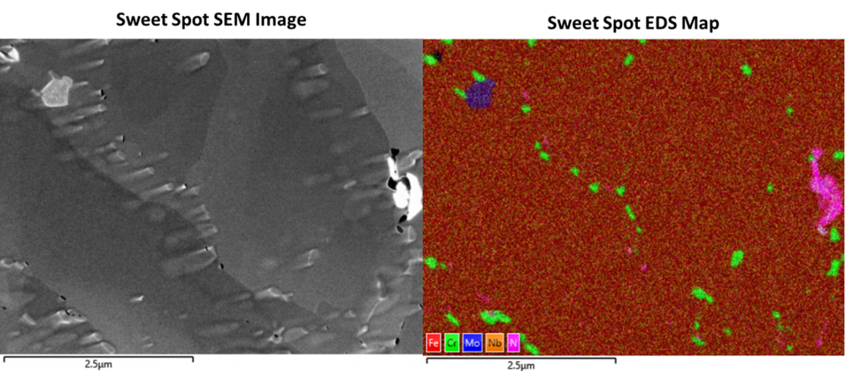
By combining ‘sweet spot’ imaging with Ultim Extreme mapping we can acquire EDS data that is truly surface sensitive, an example of which is shown in Figure 3 where surface inclusions can clearly be seen when performing imaging & EDS at 3kV with a working distance of 4mm.The chemical information from EDS mapping done in this geometry then provides greater insight into the contrast mechanisms that were previously observed in the SEM images.

Figure 3. Sweet spot imaging and EDS of inclusions in steel. EDS analysis is performed with the Ultim Extreme detector whilst the SEM is imaging at 3 KV with a working distance of 4 mm.
Learn more about how you can utilise this imaging sweet spot by watching our recent webinar with Dr Sato on the subject.
We send out monthly newsletters keeping you up to date with our latest developments such as webinars, new application notes and product updates.
 公安机关备案号31010402003473