产品
FIB-SEM
Nanomanipulators
OmniProbeOmniProbe Cryo软件
AZtec3DAZtecFeatureAZtec LayerProbeTEM
Hardware
EDSUltim MaxXploreImaging
软件
AZtecTEM
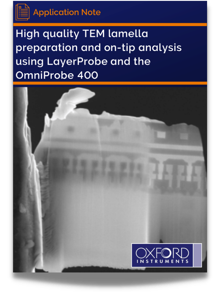
High-resolution TEM image quality is greatly impacted by the thickness of the TEM sample (lamella) and the presence of any surface damage layer created during FIB-SEM sample preparation. Here we present a new technique that enables measurement of the local thickness and composition of TEM lamellae and discuss its application to the failure analysis of semiconductor devices. The local thickness in different device regions is accurately measured based on the X-ray emission excited by the electron beam in the FIB-SEM. Examples using this method to guide FIB-SEM preparation of high-quality lamellae and to characterise redeposition are shown for Si and III-V semiconductor devices.
By downloading this application note you will see:
 公安机关备案号31010402003473