产品
FIB-SEM
Nanomanipulators
OmniProbeOmniProbe Cryo软件
AZtec3DAZtecFeatureAZtec LayerProbeTEM
Hardware
EDSUltim MaxXploreImaging
软件
AZtecTEM
 牛津仪器集团成员
04th June 2020 | Author: Dr Sam Marks
Ultim Extreme is a unique windowless EDS detector optimised to perform high sensitivity, low energy X-ray analysis and match the nanometer scale, high resolution imaging conditions of modern scanning electron microscopes (SEMs). Ultim Extreme breaks from convention by focussing on short working distance EDS, which results in enhanced image resolution and enables low kV analysis down to 1kV. This has enabled new applications in life sciences, battery materials, semiconductors and nanoscale materials analysis.
In this blog, I will outline some things to remember during day to day Extreme operation, focussing on some of the key variables that will help you get the most out of your detector. These are:
Following this advice should help you improve your detection of light elements, investigate very small structures, and generate high spatial resolution EDS maps.
For high spatial EDS, it is vital to consider the region from which X-rays are coming from and to match as closely as possible with the spatial resolution required to analyse your sample and characterise the structures of interest. The volume of interaction between the electron beam and the sample, and where X-rays are generated can be controlled by adjusting the accelerating voltage. The lower the accelerating voltage the smaller the volume of interaction, the higher the spatial resolution of analysis and smaller structures can be distinguished. Using an accelerating voltage of 20 kV, X-rays can be generated 1 µm or more away from the electron beam, if you were to analyse a 50 nm inclusion, less than 10% of the acquired EDS data would be generated by the inclusion, and you are effectively sampling mostly the bulk matrix material surrounding it. By reducing the accelerating voltage, this volume is decreased so at 3kV the majority of electron beam- sample interaction and X-ray generation would be happening within a 50nm inclusion. The examples below show Monte Carlo simulations used to calculate the region Fe Lα X-ray generation as a function of accelerating voltage.
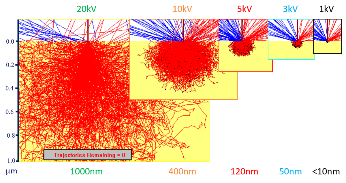
Monte Carlo simulations modelling the interaction volume for Fe X-rays generated within pure Fe for a range of accelerating voltages.
herefore, by reducing the accelerating voltage, we can improve both the lateral and depth resolution of EDS maps. The images below show a semiconductor device has been mapped using an acceleration voltage of 3 kV and 1 kV. At 1 kV, the EDS map (and associated SEM image) is more surface sensitive, with the O map resolving the structures much better and picking up little signal from the buried layers. In comparison, the 3 kV O map shows a more diffuse structure, with structure edges impossible to distinguish, it is further confused by oxygen X-rays emitted from structures deeper in the device.
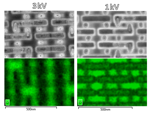
Ultim Extreme analysis of semiconductor device. Data is acquired using accelerating voltages of 3 and 1 kV to examine the effects of interaction volume on EDS data. By reducing the acceleration voltage down to 1 kV the interaction volume becomes contained within the top 10 nm of sample, X-rays are no longer generated within the buried semiconductor structure, resulting in an EDS map more representative of the surface structure.
The other important point to consider when reducing accelerating voltage to enhance spatial resolution is the energy required to excite the characteristic X-rays you need to detect. Under low kV conditions, electrons are unlikely to have the energy to excite core-shell transitions that cause high energy X-rays typically used for micro-analysis, e.g. K shell transition X-rays of transition metals and L shell transitions of heavier elements. This can be seen in the table below, which identifies the highest energy X-ray line that can be excited for a set accelerating voltage. When lowering the accelerating voltage, X-rays from the full periodic table are available down to about 1.5 kV accelerating voltage, where only X-ray from elements in the narrow range from Se to Rb are no longer excited. At 1 kV most elements can still be identified and mapped from their K, L, M or N X-rays. Periodic tables highlighting the useable X-ray lines at different accelerating voltages are available on request.
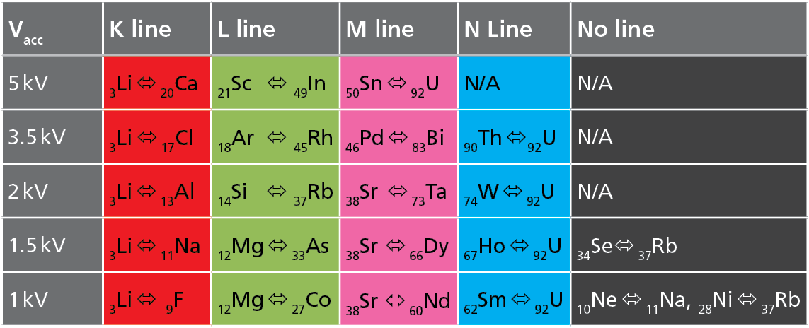
Table of highest excitable X-ray transition as a function of accelerating voltage. Elements in the no line column cannot be excited and will not produce X-rays at that accelerating voltage.
Low energy X-rays (with energy less than 1keV), are less familiar to analysts but can still provide significant useful information about the elemental make-up of samples when characterising nanostructures at low kV. For example, analysing the semiconductor structure at 1kV as shown below, means the beam energy is too low to excite SiK and WM X-rays, so low energy SiL and WN X-rays are measured instead.
Example of X-ray line substitution during low kV EDS analysis. By reducing the accelerating voltage AZtec must utilise non-traditional lines to perform EDS analysis on certain elements.
The trick is to balance the spatial resolution and the X-ray generation. My general advice is to use an accelerating voltage that is low enough to give you the spatial and surface resolution you need, but no lower, so you are exciting as many higher energy lines as possible. It is occasionally necessary to use a little higher accelerating voltage to ensure X-rays from all important elements can be detected, but as most X-ray generation happens close to the electron beam, X-ray maps often show better apparent spatial resolution than the interaction volume may suggest should be possible.
Extreme’s windowless design and large solid angle ensures maximum sensitivity for the detection of these low intensity, low energy X-ray lines.
The process time selected for EDS acquisition controls how wide the peaks appear in the spectrum. Short process times are used for high throughput analysis but for Extreme analysis where count rates are normally low, long process times should be used. Using a long process time with the best possible spectral resolution is important for low energy analysis because of the close separation and complex shapes of many of the X-ray lines detected. Therefore using a long process time, like 5 or 6, helps the software maximise the accuracy for spectrum processing needed to separate out the contributions of different elements where peaks overlap. The example below highlights the importance of utilising a long process time to ensure accurate deconvolution of complex X-ray overlaps. In this example, there is a strong overlap between the W structure and the surrounding Si structure of a semiconductor device. In the SmartMaps
, which are simple window integral maps, Si appears to be distributed throughout the sample with the Si and W maps appearing to be almost identical. By processing the data as TruMaps, we automatically apply our peak deconvolution routines, resulting in clearly defined independent W and Si structures in the sample.
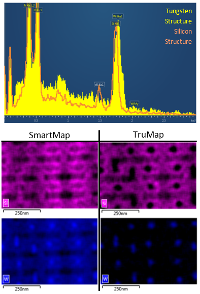
X-ray spectra collected at 3 kV from a semiconductor device with the associated Si and W SmartMaps and TruMaps. The Si Kα and W Mα X-ray lines ar 30 eV apart, requiring robust peak deconvolution software to separate the two energy lines accurately.
Hopefully this blog has given you some idea of the unique capabilities of our Ultim Extreme detector, opening new avenues of materials characterisation in fields such as life sciences, semiconductors and batteries. To discover exactly how the Ultim Extreme can aid you in your research, book a demo with one of our application specialists below.
Book a DemoWe send out monthly newsletters keeping you up to date with our latest developments such as webinars, new application notes and product updates.
© 牛津仪器 2024
 公安机关备案号31010402003473
