产品
FIB-SEM
Nanomanipulators
OmniProbeOmniProbe Cryo软件
AZtec3DAZtecFeatureAZtec LayerProbeTEM
Hardware
EDSUltim MaxXploreImaging
软件
AZtecTEM
 牛津仪器集团成员
31st October 2019 | Author: Dr Hui Jiang
In heavily regulated industries, there is a continuous requirement to limit environmental impact, reduce costs and increase safety. Optimising the materials to meet these challenges, requires detailed analysis so that the fundamental material structure and composition can be understood. In order to address these challenges in modern, fast, development environments, analytical techniques must be able to deliver fast and accurate characterisations.
Electron Backscatter Diffraction (EBSD), is an SEM based technique for microstructural characterisation. As the electron beam generated by the SEM is scanned over the surface of a crystalline sample (e.g. metals, minerals etc.), it is diffracted and generates a diffraction pattern. This pattern holds information on the crystal structure and orientation at the point on the sample where it was generated and is captured and recorded by an EBSD camera for automatic analysis. This information is recorded for each pixel in each field of view, meaning that a large dataset is formed which can be mined to extract a wealth of information including phase discrimination, grain size measurements, grain orientations, texture and strain.
When I first used EBSD back in 2001 to analyse a Ti64 alloy, the cameras were running at 50pps (patterns per second) and I thought that was fast. Since then, the EBSD technique has been constantly developed and now with our latest generation of CMOS-based EBSD detector -Symmetry, we can run at speeds of up to 3400 patterns per second, at higher levels of data quality than ever before. Analysis runs which previously took overnight or even days to complete, are often now completed on timescales of hours or minutes. With higher levels of sensitivity, even complex materials can be analysed at high speed, making EBSD a useful and practical technology for analysis in heavily regulated industries.
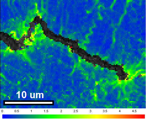
Deformation and strain within a material affects the suitability of that material for applications where structural integrity is an important consideration of component design. This means that it is very important to understand strain and deformation within materials - EBSD is an ideal technique to investigate this. Below you can see a map of a Ni superalloy sample used in aerospace industries – with considerable intragranular deformation. Here, we have used EBSD to visualize the location and local gradient of strain. You can see how strain levels vary around a crack, with blue showing low levels of strain and green through to red showing high levels. This sort of image is known as a Kernel average misorientation map and shows plastic strain. This map was collected at 2900 pps and took only 4 seconds to acquire – some very important information collected very quickly!
The above example was for a single field of view in the microscope but sometimes it is necessary to analyse a much larger area of a specimen. Covering such a large area of course increases the time that an analysis will take – potentially to many hours. In the past when I went to setup a run like this – sometimes to be left overnight, I always worried that something could go wrong over such a long duration, e.g. sample drifting, beam instabilities, or even whether I had set up a suitable area of analysis. With the speeds that we can now achieve with the Symmetry detector, these considerations are no longer a source of worry. Below is an example from a dissimilar metal weld in an automotive component - the map shows the interface between the martensitic 9Cr steel and the FCC weld metal. Here, we wanted to examine a wide transect but at sufficient resolution to resolve the small grains, as these features may have an effect on the mechanical properties of the material. The map was collected at 3000 pps with diffraction patterns collected and analysed from 4 million points in ~20 mins. The bimodal grain size distribution is clearly visible.
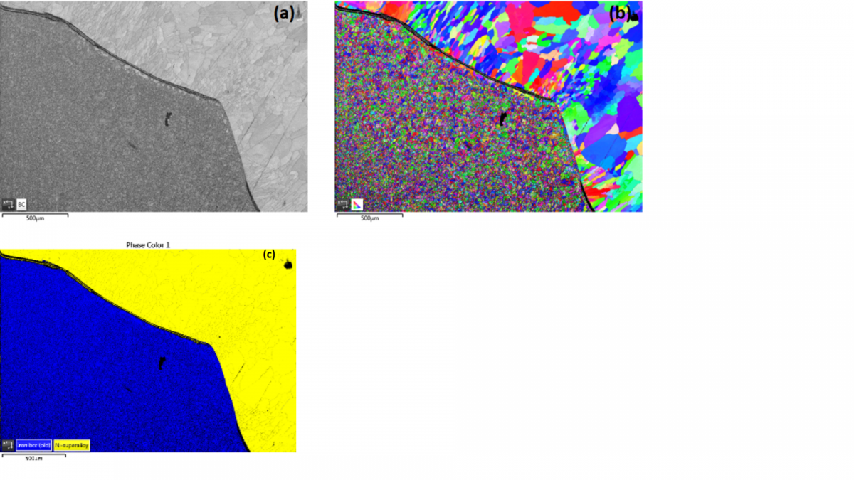
EBSD (a) band contrast, (b) orientation map and (c) phase map of interface between the martensitic 9Cr steel and the FCC weld metal.
The capabilities of the Symmetry EBSD system mean that rapid, accurate analyses can be performed in the short time to get the answers that are needed in materials development and quality monitoring, in a way that was never previously possible.
To find out more, watch our recent webinar that highlights materials development in highly regulated industries such as automotive and aerospace with real world examples from WMG and Intertek.
We send out monthly newsletters keeping you up to date with our latest developments such as webinars, new application notes and product updates.
© 牛津仪器 2024
 公安机关备案号31010402003473